

Technology is changing fast. One important part of this change is the use of patterned silicon wafers. These wafers are thin slices of silicon that have special designs on them.
They help make many of the devices we use every day, like smartphones and computers. In this blog, we will explore how patterned silicon wafers are important for future technology. We will look at their role in semiconductors, artificial intelligence, and nanotechnology.
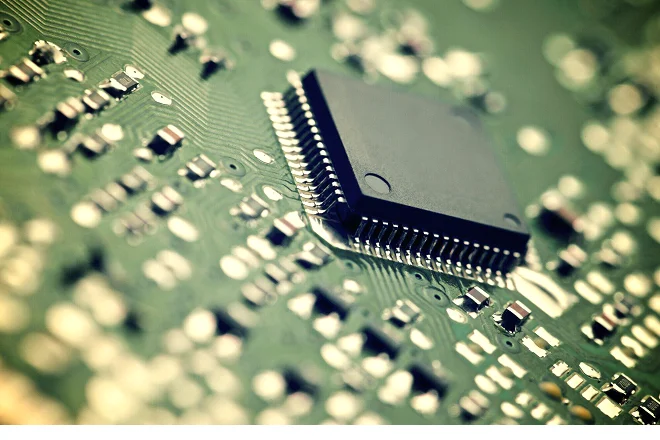
What are Silicon Wafers?
Silicon wafers are flat pieces of silicon. They are usually round and very thin. These wafers are made from pure silicon, which is a common element found in sand.
Silicon is a great material for making electronic devices. It can conduct electricity and is very stable. This makes it perfect for creating the tiny parts inside computers and other gadgets.
Patterned silicon wafers have special designs on their surfaces. These patterns help to create different electronic components. The designs can be very small and complex.
This allows for more parts to fit on a single wafer. As a result, devices can become smaller and more powerful.
The Importance of Semiconductors
Semiconductors are materials that can conduct electricity under certain conditions. Silicon is the most common semiconductor used in electronics. Patterned silicon wafers are crucial for making semiconductors.
They help create the tiny circuits that power our devices. When we use patterned silicon wafers, we can make more advanced semiconductors. These semiconductors can process information faster and use less energy.
This is important for the future of technology. As we create more powerful devices, we need semiconductors that can keep up with the demand, ensuring that innovations in fields like artificial intelligence, renewable energy, and telecommunications can thrive and evolve.
Advancements in Artificial Intelligence
Artificial intelligence, or AI, is changing how we live and work. AI systems can learn and make decisions like humans. To work effectively, AI needs powerful hardware.
This is where patterned silicon wafers come in. Patterned silicon wafers help create the chips that run AI algorithms. These chips need to be fast and efficient.
With the help of patterned wafers, we can design chips that can handle large amounts of data quickly. This allows AI to perform tasks like recognizing faces or understanding speech, ultimately enhancing our daily experiences and driving innovation across various industries.
The Role of Nanotechnology
Nanotechnology is the study of very small things, usually at the scale of atoms and molecules. This field has many exciting applications. This could lead to new materials and devices that are much smaller and more efficient.
Patterned silicon wafers are essential in this area as well. Using patterned silicon wafers, scientists can create tiny structures that can be used in various ways. For example, they can make sensors that detect changes in the environment.
These sensors can be used in medicine, agriculture, and even in our homes. The possibilities are endless when it comes to nanotechnology and patterned silicon wafers, paving the way for groundbreaking advancements that could revolutionize industries and improve our quality of life.
How Patterned Wafers by Silyb Make a Difference
One company that is making strides in this field is Silyb. The patterned wafers by Silyb help advance technology. Their wafers are designed to improve the performance of semiconductors and other electronic components.
This means that devices made with Silyb’s patterned wafers can be faster and more efficient. By using these advanced wafers, engineers can create better products. This can lead to new innovations in technology.
As we continue to rely on electronics, the role of companies like Silyb becomes even more important, driving the evolution of smart devices and enhancing our interconnected world.
Future Innovations with Patterned Silicon Wafers
As technology continues to grow, patterned silicon wafers will play a key role in future innovations. We can expect to see new devices that are smaller, faster, and more powerful. For example, wearable technology could become even more advanced.
Imagine smartwatches that can monitor your health in real time. In addition, patterned silicon wafers could help improve renewable energy sources. Solar panels made with these wafers could be more efficient.
This would allow us to harness more energy from the sun. As we face challenges like climate change, these innovations will be crucial, enabling a more sustainable future and reducing our reliance on fossil fuels.
Challenges and Opportunities
While patterned silicon wafers offer many benefits, there are also challenges. The process of creating these wafers can be complex and expensive. However, as technology advances, these processes are becoming more efficient.
This means that the cost of producing patterned silicon wafers may decrease in the future. Moreover, there is a growing demand for skilled workers in this field. As more companies invest in technology, there will be more job opportunities.
Students who study engineering and technology will find many paths to success, contributing to a workforce that drives innovation and meets the evolving needs of the industry.
The Global Impact of Patterned Silicon Wafers
The impact of patterned silicon wafers goes beyond just technology. They can also affect the global economy. As countries invest in tech development, they create jobs and boost their economies.
This can lead to better living standards for people around the world. Furthermore, advancements in technology can help solve global issues. For example, better medical devices can improve healthcare.
Improved communication technology can connect people across the globe. Patterned silicon wafers are a key part of this progress. They enable innovations that can change lives and improve our world, fostering a more interconnected and prosperous future for all.
Role of Patterned Silicon Wafers
In summary, patterned silicon wafers are vital for the future of technology. They support advancements in semiconductors, artificial intelligence, and nanotechnology. As we look ahead, these wafers will help create smaller, faster, and more efficient devices.
The role of companies like Silyb in producing these wafers is significant. They contribute to the ongoing development of technology that can enhance our daily lives. As we embrace these innovations, we can expect exciting changes in various fields.
Did you like this guide? Great! Browse our website for more!